Learning to Love
Surface Mount Technology (SMT)

Lost in
translation: Somehow ‘soldering
practice’
becomes ‘welding practice’ in advertisements for certain small
electronics
kits
from China. I first practiced ‘welding’
surface mount devices (SMD) with two Gikfun kits:
flashing LEDs and infrared radar
(proximity sensing), each costing less than
$10. For the first kit I
used a fine-tipped
soldering iron and small diameter wire solder. The work was
challenging, especially the soldering of integrated circuit components,
but not
impossible. (The photos above are from product advertisements—not my
solder practice!) A circular pattern of flashing LEDs rewarded
successful
completion of the first kit (left in photo). In fairness, the kit makes good on its promise of soldering practice, although as a finished product it would not likely sustain long term interest.

 More
hot
air: Before undertaking the second SMD practice exercise I
had acquired an Aoyue SMD Rework Station, along
with paste type solder, which is applied to the PCB (or stencil) by
squeezing from a syringe.
Through trial-and-error I zeroed-in on a temperature and airflow combination
that
melted solder without blowing the tiny components into the carpet, provided the
air flow nozzle was held at a suitable distance and angle with respect to
the target devices. For what it’s worth, the experimentally determined temperature was
225°
C. I cannot specify airflow rate meaningfully, because neither the Rework Station
nor its instruction manual identifies units for the
displayed air pressure
numbers—Air flow
was 15 something, units unknown.
More
hot
air: Before undertaking the second SMD practice exercise I
had acquired an Aoyue SMD Rework Station, along
with paste type solder, which is applied to the PCB (or stencil) by
squeezing from a syringe.
Through trial-and-error I zeroed-in on a temperature and airflow combination
that
melted solder without blowing the tiny components into the carpet, provided the
air flow nozzle was held at a suitable distance and angle with respect to
the target devices. For what it’s worth, the experimentally determined temperature was
225°
C. I cannot specify airflow rate meaningfully, because neither the Rework Station
nor its instruction manual identifies units for the
displayed air pressure
numbers—Air flow
was 15 something, units unknown.
Then
what? Without giving it thought
I had imagined that after the solder practice stage,
other
SMT kits would be available, not just for learning to work with surface mount
devices, but to make useful or interesting products on completion. I
had in mind an end result that would be richer
than flashing LEDs, not necessarily a big-screen TV, but somewhere between the extremes of solder practice kits
and manufactured electronics. Far as I can tell, no such
thing exists. Kits that include SMT components usually have those elements
pre-installed, with only through-hole components or socketed IC’s left
for
the builder to install. It appeared for a while as if the Rework Station would
gather dust,
which from time to time could be heated up and blown away (its self-cleaning feature). —But then
another
thought occurred..
Homebrew
SMT:
If kits of the type I imagined are uncommon, why not
convert one of my previous projects to SMT, or create an SMT project
from scratch. At this point I was unsure whether it would be
possible to purchase surface mount versions of popular op amps or
timers or
TTL, etc., in small quantities and at reasonable cost. What if such
components were only to be had in factory quantities? It would be crazy
to consider buying a thousand 555's in order to make one timer.
However, a quick Internet search confirmed that common SMDs can be
purchased in small
quantities from
companies like Mouser
or Digikey.
Since such components are small, and almost lighter than air, shipping
costs
are also reasonable.
Hidden
Advantage: From the amateur experimenter’s perspective, it
is important to keep the cost of projects as low as possible. Companies
that develop products for profit can afford to invest in advanced design software or sophisticated
hardware; whereas
amateurs or
students are generally obliged to pursue their interests
within stricter budgetary
constraints.
This thought led to an epiphany of sorts. You get more for
less with SMD than with the older more familiar
technology! The first such economy-of-scale poked through to
my awareness in relation to the circuit board design phase.
The non-commercial (free) version of Autodesk Eagle supports PCB
layouts of up
to 80 cm2, or nominally 80 mm × 100 mm. As a
guess, twice as much
circuitry can be packed onto this small design area using SMD than
using through-hole or socketed components.
This comparison is based
on circuits that are familiar to me—in other words,
amateur designs. LSI and multi-layer boards would boost component density to a much higher level.
Picking
a
project: I didn’t immediately think of a novel idea for a
first homebrew SMT project. But one of my previous projects
included six DIP ICs (TTL). That same project also involved a small
number of resistors,
capacitors and LEDs. If redesigned for SMD, the project would be
significantly smaller, and should easily fit within an 8 cm ×
10 cm layout. Later I
came to realize that the close spacing of solder pads for
SMD IC’s, and the fact that they are all on the top PCB layer,
made
routing of connections more challenging. —Eagle
has an automatic routing feature, but I have not tried it. Manual
routing,
or at least my
manual routing is
very non-optimal. It relies on a great many vias. For this
prototype SMD project I placed each part as soon as it
was added to the schematic, and routed the traces (wires) that were
possible to route at that time. I did not draw the full schematic and place all
parts
before
starting to route connections. This one-part-at-a-time approach likely
contributed
to the large number of layer crossings (vias).
Boards:
I had ordered PCBs from JLCPCB before, and been entirely satisfied. CAM files were uploaded on Thursday and manufactured boards
(quantity 5) delivered the following Wednesday, China to Eastern US in 6 days,
including manufacture—Amazing! (This is not an advertisement.. I have
no connection to JLCPCB except as a customer.) Components that were not
on-hand (chiefly the TTL IC’s) were ordered concurrently from other
sources.

Solder
Practice Redux: It may be premature to claim having
improved my SMD soldering technique through practice with this first homebrew SMD project, but here goes.
After trying a few different approaches, one of which caused solder to pool
under the chip—definitely not good, I hit upon a method that
appeared to work
better than others. First the IC was positioned over the bare pads, and
in
the correct orientation for soldering. With the chip in position I
applied heat from a few centimeters height above one corner. This
warmed the board in the area to be soldered. Then I just touched the
heated part with solder paste—the heated board caused the paste to
liquefy and flow along the two or three pads/tabs to be soldered. Heat
was
again applied from above, this time for long enough to melt the solder
and cause it to flow onto the tabs, thus securing the IC at one corner.
Next I repeated the process on the opposite corner. By then
the board was generally hot enough to liquefy the paste, without the
necessity of applying additional heat. After the diagonally opposite
corner was secured I returned to the first side, and similarly soldered
the remaining pins, starting on the end away from the first
application. Finally I soldered the remaining pins. All connections were
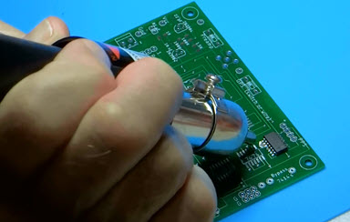
shiny, with no excess or solder bridges. I used this method for all 6 ICs on
the third board belonging to this project. An inset toward the
end of the video demo (see link below) illustrates this process. It was by
far the
cleanest of several tries. No resoldering was needed.
I should clarify that on a previous board I had
applied cold paste in greater quantity, and afterward had to desolder
several ICs, clean the board, and
resolder them. Another practice board was fine electrically, but not as
clean as the
one soldered using the technique outlined in the preceding paragraph.
Of course, proper equipment, including a stencil frame and oven would
surely produce the same or a better result. However, when a hot air
reflow station is the only tool available, it remains possible to
solder SO-14 or SO-16 footprint ICs very cleanly—perhaps, as in my
case, by substituting patience for experience.
Acknowledgements:
Although the GPS
Frequency Counter project in its original
form has been described on a separate page, I want to reacknowledge key
sources that contributed to the concept. First, the
idea of
using a GPS to define the counting interval came from the QRP
Labs QCX transceiver kit, and subsequent correspondence with
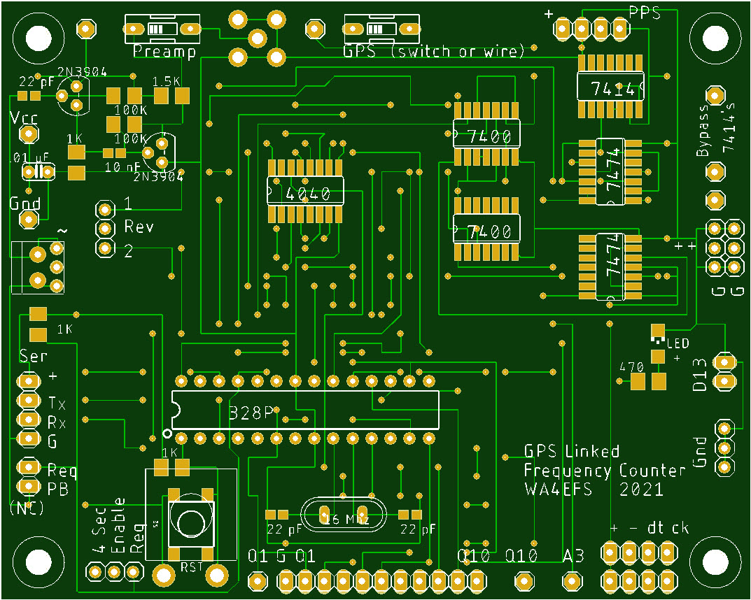
its designer Hans Summers G0UPL. The preamplifier circuit (upper left
corner of PCB) came from the Four
State QRP Group Frequency Mite kit, designed by Dave Benson
K1SWL. I have included the revised schematic above (i.e., the SMD
version of
the project). For more detail please refer to the original write-up (non SMD
version). Finally the microcontroller sketch for the project described
on this page may be found here.
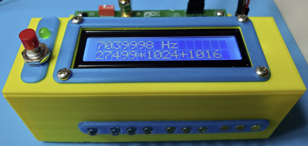
Demo video: Learning to
Love SMT
Project descriptions on this page are intended for entertainment only.
The author makes no claim as to the accuracy or completeness of the
information presented. In no event will the author be liable for any
damages, lost effort, inability to carry out a similar project, or to
reproduce a claimed result, or anything else relating to a decision to
use the information on this page.
