AD9834 DDS
(Part 1):
I have separately described a project based on the Analog Devices
AD9850 chip (see AD7C
VFO
write-up). The following paragraphs are about how to figure out
and test another DDS
chip, the AD9834.
The
board shown on the right in the illustration above was purchased on
eBay. It is similar to this one, with three SMA jacks
labeled Sine1, Sine2, and Square. The AD9834 chip is well-documented in
the Analog
Devices datasheet and related application note. For example,
AN-1070 by Liam Riordan explains how to compute and load a
frequency into one of the chip’s frequency select registers. However,
there
seem to be few completely documented applications for this chip, and
none that I could find referencing the specific evaluation board I
purchased. The
small mail packet from China included only the board—no schematic or
other documentation.
 The PCB connector labels (left) were a mixture of familiar and
unfamiliar
terms. Power connections and SDA / SCK were familiar,
and
The PCB connector labels (left) were a mixture of familiar and
unfamiliar
terms. Power connections and SDA / SCK were familiar,
and RST for ‘reset’
was meaningful, although I didn’t
know what to do with it. I still do not know what
the abbreviations PS and PSY stand for, although I was able to deduce
what to do with one of them. By tracing AD9834 pin 15 on the circuit
board, I found that the chip’s
FSYNC (datasheet page 9) goes to the header pin labeled PSY.
RST for ‘reset’
was meaningful, although I didn’t
know what to do with it. I still do not know what
the abbreviations PS and PSY stand for, although I was able to deduce
what to do with one of them. By tracing AD9834 pin 15 on the circuit
board, I found that the chip’s
FSYNC (datasheet page 9) goes to the header pin labeled PSY.
Correction:
A correspondent informed me that what I had read as ‘PSY’
was actually ‘’FSY’.
Mr. Glen Wilson very kindly sent the following corrected figures, and
explained the abbreviations that had puzzled me.
According
to Mr. Wilson, “The Fselect pin is used for FSK modulation. Low selects
one of the pre-programmed frequencies as stored by the Arduino program;
a high will send the other. Pselect is similar [but] selects different
phases for PSK modulation.” This explanation eliminates the confusion I
expressed in the preceding paragraph. Unfortunately the block diagrams
in the second part of this article (below) also include the erroneous
‘PSY’ annotation.
 Many hours went down the tubes in a variety of failed attempts to
communicate with the AD9834 before I came across a tremendously useful
test sketch authored by Alexander C. Frank, and originally written for
the AD9833. The sketch may be found near the bottom of this page.
Many hours went down the tubes in a variety of failed attempts to
communicate with the AD9834 before I came across a tremendously useful
test sketch authored by Alexander C. Frank, and originally written for
the AD9833. The sketch may be found near the bottom of this page.
The PCB master clock frequency is
stamped on the crystal (photo left). To adjust
Mr. Frank’s program for
this clock frequency is a
trivial one-line edit. That is in fact the only
thing I changed in the sketch. The wiring is also simple, once it was
clear which pin
was FSYNC (table above). One other very minor clarification...
Mr. Frank’s
Arduino sketch uses serial COM for user input. When entering a
test frequency and waveform type via the serial device use ASCII
10 (newline) as the
command terminating character.
Generated sine and triangular waves are
output via the Sine1 jack, while square waves are output via the
top-mounted jack. The oscilloscope probe was capacitively coupled for
the test sine wave shown above (7.036 MHz), but directly coupled for
the other two examples (100 KHz square wave and 5 KHz
triangular). In other words, while the Square wave output is centered
on 0 volts, the triangle (via Sine1) is centered on half its P-P
voltage, and the sine output would be also if the probe were not
capacitively coupled.
The drop-off in output with increasing
frequency is greater than I recall seeing from the AD9850. Above 30 MHz
the signal is messy, and hardly measurable. Of course, these readings
reflect breadboard wiring, with a 2200 ohm load resistor. A better
result might be expected from an improved test setup.
AD9834
DDS Demo: RTTY.mp4
AD9834 DDS and FSK (Part 2):
The above demo
video introduces something that was not discussed in the accompanying
write-up, viz
an Arduino application called TinyFSK written
by Andrew Flowers K0SM. Two Arduino Nanos were used for the demo, one
running TinyFSK and the other to control the AD9834. Outputs of the FSK
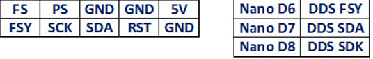
Arduino connect to inputs of the AD9834 controller, as shown in the
diagram below.
It occurred to me
that the two programs (sketches)
could be combined and that one Nano would suffice for both FSK and
controlling the DDS. Blending the two programs turned out to be easier
than expected. Starting with TinyFSK, I imported just enough AD9834
control code to generate a sine wave for a specified frequency, and
then inserted calls to update the frequency at
each place where TinyFSK writes to a DIO pin.
It was unclear at first how to turn transmit OFF, but specifying 0 Hz
for the frequency worked! There
was no memory crunch, so no need to remove TinyFSK’s
DIO writes (FSK_DDS.ino).
For
the audio FSK
demonstration in the first part of the preceding video, output from the
DDS was fed to the computer sound card line-in jack. In the second part
of the video, the AD9834 was configured to generate RF at 7.1 MHz (+
FSK offsets). According to my calculation, output power was less than 1
milliwatt. However for this demo, transmit and receive antennas were
only about 50 feet apart.
The video does not
include an intermediate test in which an RTL dongle and SDR were used
to receive RF from the DDS. For this exercise, the receive antenna was
a length of wire hanging over the stairwell, no more than 10 feet from
the transmit antenna!
In the screen capture image, Termite
(lower left)
keys the FSK Arduino. On the right SDR# receives the 7.1 MHz signal.
Finally, MMTTY (upper left) decodes the
SDR’s audio output.
Observe that decoding lags a couple of characters behind the sender.
All this started as a small-scale
exploration of the
AD9834. I never intended to get into FSK, and certainly not to go
further than encoding and decoding a signal, but sometimes it
is hard to stop, even when one’s
better judgement screams ‘enough already’. Thus,
in a roundabout way I became curious about how to amplify DDS-generated
RF output. Although
the Arduino connection diagrams (above) include the legend ‘to
amplifier’, none of the demos involved an amplifier. At some point I
wondered whether DDS output could be boosted sufficiently to drive the Pacific
Antenna 10-watt linear amplifier.
That would mean increasing the output to a few hundred milliwatts at
least. Unfortunately I
know almost nothing about RF amplifiers.
An obvious next step was to examine a few example low-power RF
circuits, such as the Pixie or the One-Watter (both described near the
top of this page). I also found a couple of circuits on the Internet
covering the power range of crystal oscillator to fractional-watt
output. Although
differing in detail, these reference circuits exhibit common features,
which I attempted to understand and duplicate.
A little bit of experimentation
with different components or values and two
stages of amplification eventually
led to a potentially exploitable result. RF output measured
about
3 volts P-P across a 50 ohm resistor. So far so good, although the
second stage transistor got very hot. To
address
the heat problem, I fabricated a heat sink from aluminum bar stock and
a ring terminal. (The idea of using a ring terminal for bonding the
heatsink to the TO-92 came from the Pacific Antenna QRP amplifier
project, where a ring terminal is used to draw heat from a diode.)
Loose wires are the bane of breadboard construction—the greater the
component count the more likely it is that something will work loose.
So it was with the amplifier. Sometimes it worked and sometimes not, so
I reconstructed the circuit on a generic PCB, more or less the same as
it was, adding a PTT relay and some test points.


 Sometime later a transistor lead broke due to the heatsink bending
whenever the board was turned over, or from accidentally setting my
coffee cup on it. When this happened, I unsoldered the transistors and
installed 3-hole headers so that the transistors could be easily
replaced or exchanged for different values, etc. But that was later.
First I hooked the PCB preamplifier to the 10-watt linear.
Preamplifier output was not up to the linear’s minimum spec., but
“nothing ventured nothing gained.”
Sometime later a transistor lead broke due to the heatsink bending
whenever the board was turned over, or from accidentally setting my
coffee cup on it. When this happened, I unsoldered the transistors and
installed 3-hole headers so that the transistors could be easily
replaced or exchanged for different values, etc. But that was later.
First I hooked the PCB preamplifier to the 10-watt linear.
Preamplifier output was not up to the linear’s minimum spec., but
“nothing ventured nothing gained.”
The entire test setup consisted of the DDS and control Arduino (still
on breadboard), the amplifier PCB, the linear, an MFJ-971 QRP tuner
(for the meter), and a 10 watt resistive dummy load (not the wire wound
resistor shown in the breadboard photo). The linear has a
transmit relay keyed by RF and there was barely enough RF to
key
it. In fact, transmit keying was not consistent. Sometimes it keyed and
sometimes it didn’t.
When fortune smiled, the tuner meter
moved. Yes I know it is ugly, but however
that may be, in my world when the meter moves the experiment must count
as a success! Of course,
something is not right. How
could a resistive load reflect a third of the power? A possible clue is
that RF signal quality degrades significantly when the PCB
amplifier is connected to the linear (with the latter powered on). To
investigate further I have ordered a few bigger transistors, with a
view to adding a third stage to the preamplifier.
(To be continued, maybe...)
Footnote: One
of the routine ‘smoke tests’ carried out during construction produced
actual smoke. This does not happen often and was therefore especially
gratifying, although an acrid smell lingered for several hours
afterward.
Project descriptions on this page are intended for entertainment only.
The author makes no claim as to the accuracy or completeness of the
information presented. In no event will the author be liable for any
damages, lost effort, inability to carry out a similar project, or to
reproduce a claimed result, or anything else relating to a decision to
use the information on this page.